
|
Góc kiến thức về bán dẫn Vật liệu bán dẫn là gì? Quy trình sản xuất bán dẫn |
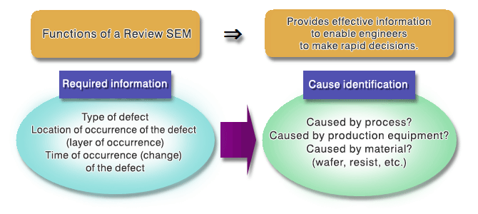
A Defect Review Scanning Electron Microscope (Defect Review SEM) is a Scanning Electron Microscope (SEM) that is configured to review defects found on a wafer. A defect detected by a semiconductor wafer defect inspection system is enlarged using an SEM to a high magnification image so that it can be reviewed and classified. A Defect Review SEM is mainly used together with the inspection systems in the production lines of electronic devices and other semiconductors.
Review SEM generally works in the following way:
1. Wafer defects are detected using an inspection system in advance
Inspection system lists position coordinates of the defects and outputs it into a file.
2. The inspected wafer and the file of the inspection result are loaded into the Review SEM.
The defect position is determined based on the position information from the defect list. Images of the defects are then taken and stored by the SEM. Several thousand to several tens of thousand defects are detected using the inspection system, and the data is output into a file. Whether to take photos of all or some of the defects can be specified in the operation settings of a recipe.
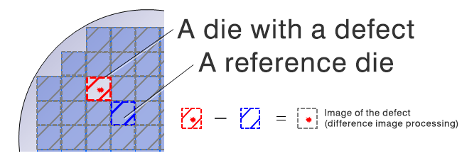
Sometimes a defect on a wafer cannot be found using the position information in the defect data file. Because of various errors, it is not easy to find a defect using the position information alone. In a defect inspection system, the defective image is compared with the adjacent die image (reference image) and the defect is detected due to the image difference (difference image processing). The Review SEM, similar to the defect inspection system, detects the defect by comparison with the circuit pattern of the adjacent die and obtains the correct position of the defect. The defect is then moved to the center of the field of view and an enlarged photo is taken of it.
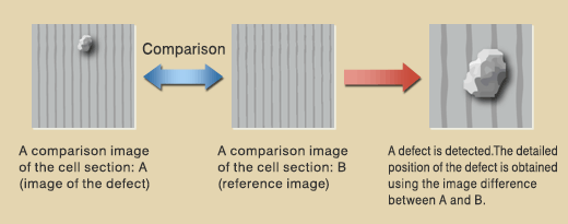
In the case of Memory IC’s defect review, in which cell patterns are arranged repeatedly, the image of the minimum unit of a cell is registered as the reference image in advance. One method of detecting a defect is to compare the image of the defect with the reference image using difference image processing. This method can speed up the defect detection because multiple sections can be compared with the same reference image.
ADR(Automatic Defect Review)
ADR stands for Automatic Defect Review. The aim of the Defect Review is to observe, classify and analyze the shape and components of the defect and particles detected by wafer inspection system in greater detail. Automatic Defect Review automatically obtains image of the desired defect using the defect information (coordinates, etc.) obtained in defect inspection. The data is stored and arranged into a database. In Defect Review SEM, an image of the defect is automatically obtained and stored using the ADR function.
ADC(Automatic Defect Classification)
ADC stands for Automatic Defect Classification. The image information of the defect stored in the image server is classified according to the cause of the defect by the classification software based on the predetermined rules and is then restored in the classification server. The classified information is sent to Yield Management System (YMS) and the host computer of the IC manufacturer so that it can be used in the failure and defect analysis. Some systems can classify defects using ADC in conjunction with the ADR function of the Defect Review SEM. The defect information obtained by ADR can also be classified collectively at a later stage.
Hitachi Multi-Purpose SEM “Inspago” RS6000 Series
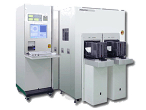
Hitachi Multi-Purpose SEM “Inspago” RS6000
Multi-purpose defect review SEM using the high-speed ADR and high accuracy ADC can be used inline to improve the yield.
It is equipped with the bare wafer automatic review function, process monitoring function and systematic defect classification function.
For more detailed product information, please click below
Hitachi Multi-Purpose SEM “Inspago” RS6000 Series
|