
|
Góc kiến thức về bán dẫn Vật liệu bán dẫn là gì? Quy trình sản xuất bán dẫn |
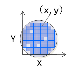
Wafer defect inspection system detects physical defects (foreign substances called particles) and pattern defects on wafers and obtains the position coordinates (X, Y) of the defects.
Defects can be divided into random defects and systematic defects.
Random defects are mainly caused by particles that become attached to a wafer surface, so their positions cannot be predicted.
The major role of a wafer defect inspection system is to detect defects on a wafer and find out their positions (position coordinates).
On the other hand, systematic defects are caused by the conditions of the mask and exposure process, and will occur in the same position on the circuit pattern of all the dies projected.
They occur in locations where the exposure conditions are very difficult and require fine adjustment.
The wafer defect inspection system detects defects by comparing the image of the circuit patterns of the adjacent dies.
As a result, systematic defects sometimes cannot be detected using a conventional wafer defect inspection system.
Inspection can be performed on a patterned process wafer or on a bare wafer.
Each of these has a different system configuration.
Below is an explanation of a typical inspection system.
Patterned wafer inspection system
There are many types of patterned wafer inspection systems, including the electron beam inspection systems, the bright-field inspection systems, and the dark-field inspection systems. Each of these has its own features, but the basic detection principles are the same.
On a semiconductor wafer, electronic devices of the same pattern are made side by side. Random defects are often caused by particles such as dust and occur in random positions, as the name suggests. The possibility that they will occur repeatedly in a specific position is extremely low.
Defects can therefore be detected by comparing the pattern images of adjacent chips (also called dies) and obtaining the difference.
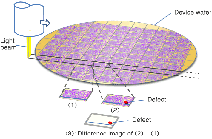
Fig.5-1. Principles of defect detection on a patterned wafer
Fig.5-1 shows the principle for detecting defects on a patterned wafer.
The pattern on the wafer is captured along the die array by electron beam or light. Defects are detected by comparison between image (1) of the die to be inspected and image (2) of the adjacent die. If there are no defects, the result of the subtraction of Image 2 from Image 1 by digital processing will be zero and no defects are detected. In contrast, if there is a defect in the image of die (2), the defect will remain in the subtracted image (3) as shown in the figure. The defect is then detected and its position coordinates are registered.
Non-patterned wafer inspection system
The non-patterned wafer inspection system is used in the wafer shipping inspection by wafer manufacturers, the wafer incoming inspection by device manufacturers and the equipment condition check using dummy bare wafers to monitor the cleanliness of equipment. The equipment condition check is also performed by the equipment manufacturer at the shipping inspection and by the device manufacturer at the equipment incoming inspection. To check the cleanliness of equipment, a bare wafer for cleanliness monitoring is loaded into the equipment and the stage inside the equipment is then moved to monitor the increase in particles.
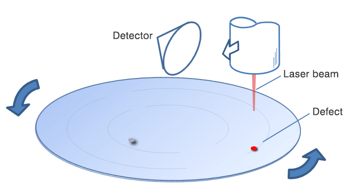
Fig.5-2. Principle of defect detection on a non-patterned wafer(1)
Fig.5-2 shows the principle for detecting defects on a non-patterned wafer.
Since there is no pattern, defects are detected directly without image comparison.
A laser beam is projected to the rotating wafer and is moved in the radial direction so that the laser beam is able to irradiate entire surface of the wafer.

Fig.5-3. Principle of defect detection on a non-patterned wafer(2)
When a laser beam is projected onto a particle/defect of a rotating wafer, the light will be scattered and detected by a detector. This detects the particle/defect. From the wafer rotation angle and the radius position of the laser beam, the position coordinates of the particle/defect are calculated and registered. Defects on a mirror wafer also include crystal defects in addition to particles.
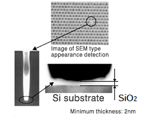
Fig.5-4. An example of detecting the residue at the bottom of a contact hole
In general, the bright-field inspection system is intended for the detailed examination of pattern defects. On the other hand, the dark-field inspection system can detect at high speed and is intended for the defect inspection of a large number of wafers.
In the electron beam inspection system, electron beam is irradiated onto the surface of the wafer, and the emitted secondary electrons and backscattered electrons are detected.
Moreover, the electron beam inspection system detects the amount of the secondary electrons as an image contrast (voltage contrast) according to the conductivity of the device’s internal wiring. If the conductivity at the bottom of the contact hole of the high aspect ratio is detected, the SiO2 residue of ultra-thin thickness can be detected.
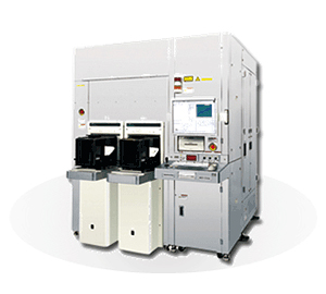
Hitachi Dark Field Wafer Defect Inspection System IS Series
Hitachi Dark Field Wafer Defect Inspection System IS Series
A next-generation dark field wafer defect inspection system capable of high sensitivity detection and high throughput inspection can monitor products at high speed, improve yield and reduce production costs. The system offers user-friendly operation with recipes prepared by simple parameter settings.
For more detailed product information, please click below.
Hitachi Dark Field Wafer Defect Inspection System IS Series
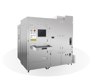
Hitachi Wafer Surface Inspection System LS Series
Hitachi Wafer Surface Inspection System LS Series
A next-generation wafer surface inspection system detects particles and defects on the surface of a non-patterned wafer with high sensitivity.
For more detailed product information, please click below.
Hitachi Wafer Surface Inspection System LS Series
|