
|
Semiconductor Room What are semiconductors? Semiconductor manufacture |
A semiconductor chip is an electric circuit with components such as transistors and wiring are formed on a semiconductor wafer. The layout of the components is patterned on a photomask (reticle) by computer and projected onto a semiconductor water in the manufacturing processes described below.
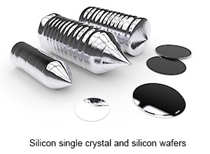
In the manufacturing process of IC, electronic circuits with components such as transistors are formed on the surface of a silicon crystal wafer.
Basics of integrated circuit formation
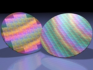
In the process of the integrated circuit creation, there are inspection and measurement steps to check whether or not the patterns are fabricated as designed. If defects are found, the fabrication will be interrupted to remove the defects from the process and to make small changes in the fabrication conditions for correction purposes. More than one hundred semiconductor dies are fabricated on a single wafer. At present, the largest silicon wafer is 300mm in diameter. Semiconductor manufacturers are looking into 450mm diameter silicon wafers for use in the future.
Semiconductor devices are completed through the front-end process (wafer processing operation) and the back-end process (assembly process) described below. (In the following description of the element process, a very small area of a wafer surface is magnified and shown schematically.)
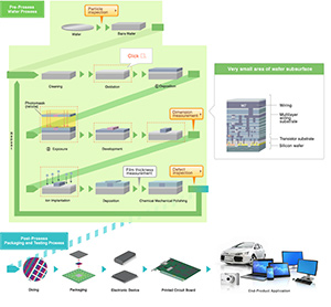
Front-end process and back-end process
|