
|
Semiconductor Room What are semiconductors? Semiconductor manufacture |
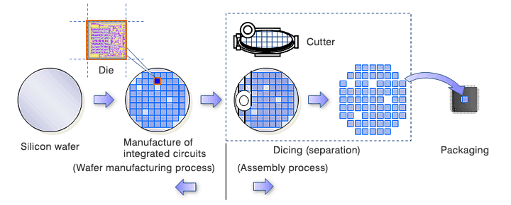
Metrology and inspection are important for the management of the semiconductor manufacturing process. There are 400 to 600 steps in the overall manufacturing process of semiconductor wafers, which are undertaken in the course of one to two months. If any defects occur early on in the process, all the work undertaken in the subsequent time-consuming steps will be wasted. Metrology and inspection processes are therefore established at critical points of the manufacturing process to ensure that a certain yield can be confirmed and maintained.
What is metrology in the processing steps of semiconductor wafers?
It is the measurement of the line width and hole diameter of a circuit pattern at
a specified location of a wafer (CD-SEM).
Measurement of the thickness of thin films on the surface of
wafers (ellipsometer, etc.)
Metrology system to check the accuracy of the
overlay(overlay metrology tool)
Metrology generally means a method of measuring numbers and volumes, mainly by using equipment.
Metrology, though often considered synonymous with measurement, is a more comprehensive concept that refers not only to an act of measurement itself but to measurement performed by factoring in errors and accuracy, as well as the performance and mechanisms of equipment. If pattern measurements are not within a given specification range, a manufactured device does not operate as designed, in which case the exposure transfer of the circuit patterns may be reworked.
The number of measurement points varies by semiconductor device manufacturer or device.
Metrology is undertaken according to the following sampling method:
-10 to 100 points for one die*
- 5 to 20 dies taken from one wafer
- 1 to 2 wafers taken from one lot (25 wafers).
Newly designed devices may go through several thousand metrological processes for one wafer during the start-up period of manufacture.
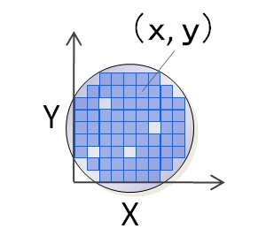
It involves the use of inspection equipment to check for compliance or non-compliance, as well as abnormality or unsuitability, in terms of specific criteria. It is a process for detecting any particles or defects in a wafer. Specifically, it is aimed at finding the position coordinates of defects (X, Y). One of the causes of defects is the adhesion of dust or particles. It is therefore not possible to predict where defects will occur. If numerous defects occur on the surface of a wafer, the circuit patterns are not created correctly, causing patterns to be missing. If there are numerous defects, they prevent the electronic circuit from operating correctly, thereby making the wafer a lot-out* product as a defective product. Detecting defects and specifying their locations (position coordination) are the primary role of inspection equipment.
|