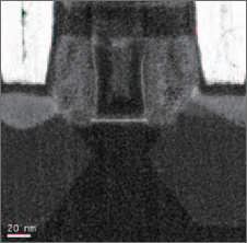
High resolution STEM imaging
HAADF-STEM image 0.136 nm, FFT image 0.105 nm (HR lens*)
BF STEM image 0.204 nm (w/o Cs-corrector)
High-speed & high-sensitivity EDX analysis: Probe current × 10 times
Elemental mapping in more rapid timely manner Low-concentration element detection
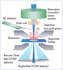
Hitachi in-house Cs-corrector
Equipped with a probe-forming spherical aberration corrector developed by Hitachi,
the automatic aberration correction process takes short time and does not need pre-experience for aberration correction.
Seamless solution from sample preparation to observation & analysis.
Holder compatibility with Hitachi FIB
|
Items |
Description |
||
|
w/o Cs-corrector |
w/ Cs-corrector |
||
|
Image resolution |
0.204 nm guaranteed (at a magnification of |
0.136 nm guaranteed (HAADF-STEM image) |
|
|
Magnification |
×100 - ×10,000,000 |
||
|
Accelerating voltage |
200 kV, 120 kV *, 80 kV* |
||
|
Imaging signal |
Bright field STEM: Phase contrast image (TE image) |
||
|
Electron optics |
Electron source |
Schottky emitter (w/o Cs-corrector) |
|
|
Cold field emitter (w/Cs-Correcter,w/o Cs-corrector) |
|||
|
Illumination lens system |
2-stage condenser lens |
||
|
Cs-corrector* |
Mullipole transfer lens design |
||
|
Scanning coil |
2-stage electromagnetic coil |
||
|
ZC collection angle control |
Projector lens design |
||
|
Electromagnetic image shift |
±1 µm |
||
|
Specimen stage |
Specimen movement |
X/Y = ±1 mm, Z= ±0.4 mm |
|
|
Specimen tilt |
Single-tilt holder: ±30° (Std. lens), ±18° (HR lens) |
||
Cs-corrected SEM imaging
The Hitachi HD-series dedicated STEM is equipped with a secondary electron (SE) detector as standard configuration; this enables imaging the
specimen surface directly in addition to obtaining interior structural information of specimen via the transmitted electron beam. SE imaging offers
fine dimension measurements of thicker samples not compatible with STEM. Spherical aberration correction pushes the SEM resolution to an
unprecedented, true atomic level.
 |
 |
Large solid angle EDS detector
analysis in a shorter data acquisition time.
Semiconductor MOS transister EDS mapping Instrument: HD-2700B(non Cs-corrected), Acquisition time:10sec./frame, Playback speed:5×
Hiện tại chưa có ý kiến đánh giá nào về sản phẩm. Hãy là người đầu tiên chia sẻ cảm nhận của bạn.