Coating of samples is required in the field of electron microscopy to enable or improve the imaging of samples. Creating a conductive layer of metal on the sample inhibits charging, reduces thermal damage and improves the secondary electron signal required for topographic examination in the SEM. Fine carbon layers, being transparent to the electron beam but conductive, are needed for x-ray microanalysis, to support films on grids and back up replicas to be imaged in the TEM. The coating technique used depends on the resolution and application.
Limited or non-conductive material samples (ceramic, polymers…etc) require carbon and/or metal coating. Cryogenic samples are freeze fractured, coated with metal (Leica EM ACE600 freeze fracture and Leica EM VCT100) and imaged in a cryo SEM.
The formvar covered TEM grids need to be coated with carbon to be conductive. Grids are treated with glow discharge otherwise solutions would not stick and distribute onto the grid. Freeze fractured samples are coated in a low angle with metal followed by a carbon backing up film (Leica EM ACE600 freeze fracture and Leica EM VCT100 or Leica EM BAF060) to produce a replica which can be imaged in a TEM.
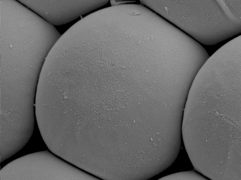
Sputter coating for SEM is the process of applying an ultra-thin coating of electrically-conducting metal – such as gold (Au), gold/palladium (Au/Pd), platinum (Pt), silver (Ag), chromium (Cr) or iridium (Ir) onto a non-conducting or poorly conducting specimen. Sputter coating prevents charging of the specimen, which would otherwise occur because of the accumulation of static electric fields. It also increases the amount of secondary electrons that can be detected from the surface of the specimen in the SEM and therefore increases the signal to noise ratio. Sputtered films for SEM typically have a thickness range of 2–20 nm.
Benefits for SEM samples sputtered with metal:
The thermal evaporation of carbon is widely used for preparing specimens for electron microscopy. A carbon source – either in the form of a thread or rod is mounted in a vacuum system between two high-current electrical terminals. When the carbon source is heated to its evaporation temperature, a fine stream of carbon is deposited onto specimens. The main applications of carbon coating in EM electron microscopy is X-ray microanalysis and specimen support films on (TEM) grids.
Metal and carbon can be evaporated. E-beam coating gives the finest layers, is a very directional process and has a limited surface of coated area. Electrons are focused on the target material which is heated and further evaporated. Charged particles are removed from the beam. Therefore a very low charged beam is hitting the sample. Heat is reduced and the impact of charged particles on the sample is reduced. Only a few runs are possible then the source has to be reloaded and cleaned. Usually, e-beam is used where either directional coating is necessary (shadowing and replicas) or fines layers are required.
Freeze fracture includes a series of techniques that reveal and replicate internal components of organelles and other membrane structures for examination in the electron microscope. Freeze etching removes layers of ice by sublimation and exposes membrane surfaces that were originally hidden.
Freeze drying, also known as lyophilization, removes water from a frozen sample under high vacuum conditions (sublimation). The result is a dry and stable sample which can be imaged in the electron microscope.
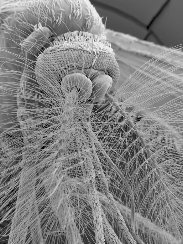
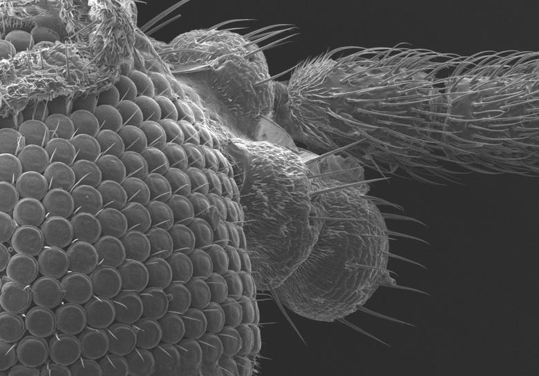
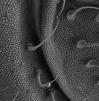
Fig. 1: Mosquito antenna (courtesy of Dr. Daniela Gruber, Vienna, Austria)