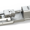


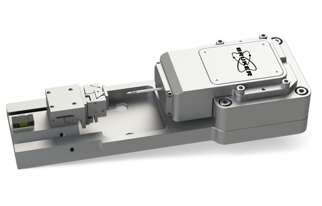
Hysitron PI 85E
Extended range in-situ nanomechanical testing instrument for scanning electron microscopes
Liên hệ
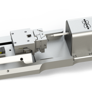
Hysitron PI 85E SEM PicoIndenter
The Hysitron PI 85E SEM PicoIndenter extends the range of your in-situ mechanical testing, bridging the gap between nanoscale and microscale characterization. This depth-sensing nanomechanical test system is specifically designed to leverage the advanced imaging capabilities of scanning electron microscopes (SEM, FIB/SEM, PFIB) while simultaneously performing quantitative nanomechanical testing. Its extended force range enables researchers to accurately test dimensionally large and/or hard structures that require larger loads to induce failure and/or fracture. The PI 85E instrument offers indentation, compression, tension, and fatigue testing across the entire materials spectrum (from metals and alloys to ceramics, composites, and semiconductor materials). The compact, low-profile architecture of PI 85E makes it ideally suited for small-chamber SEMs, Raman and optical microscopes, beamlines, and more.
Nanoindentation: High-Precision In-Situ Mechanical Testing

Characterize hardness, creep, stress relaxation, elastic modulus, and fracture touhgness of near-surface features, interfaces, localized microstructures, and thin films.
Behavior Exploration with Extended Range

Deformation of carbon nanotube (CNT) structure.
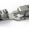
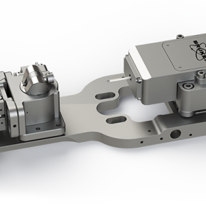
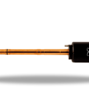
Hysitron PI 85E incorporates a variety of testing modes to characterize fundamental mechanical properties, stress-strain behavior, stiffness, fracture toughness, and deformation mechanisms across a wide range of samples. In addition to Bruker’s industry-standard testing transducer, PI 85E offers higher load (250 mN) and larger displacement (150 µm) capabilities. The high-bandwidth transducer and flexure with advanced control electronics fully optimize large-scale sample testing and provide exceptional performance and sensitivity.
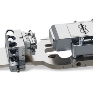
Characterization of One-, Two- and Three-Dimensional Nanostructures

Deformation of ZnO nanowire mounted on E-PTP.
The Hysitron PI 85E system uses patented Push-to-Pull (PTP) devices to characterize one-dimensional structures, such as nanowires and nanotubes, and two-dimensional structures, such as free-standing thin films. These structures can also be electrically characterized with the instrument’s optional Electrical Push-to-Pull devices. The larger displacement range of PI 85E is also ideal for testing deformation of three-dimensional lattices to larger strain.
Sản phẩm tương tự
Liên hệ
Liên hệ
Liên hệ