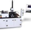


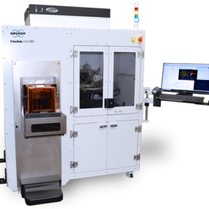
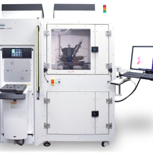
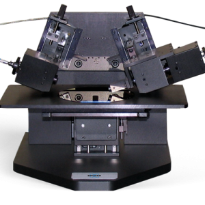
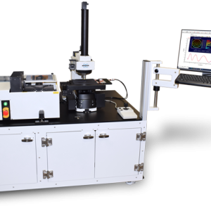
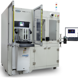
FilmTek 2000 PAR-SE
Spectroscopic reflectometry for thickness measurement of thin to very thick films on micron-sized device features
Liên hệ
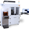
FilmTek 2000 PAR-SE
Combining patented Multi-Angle Differential Polarimetry (MADP) and Differential Power Spectral Density (DPSD) technology, the FilmTek™ 2000 PAR-SE utilizes multi-angle and multi-modal data collection to independently measure film thickness and index of refraction. By independently measuring index and thickness, the FilmTek 2000 PAR-SE is far more sensitive to changes in films, particularly films within multi-layer stacks, than existing metrology tools that rely on conventional ellipsometry or reflectometry techniques. The FilmTek 2000 PAR-SE is a fully-integrated package, paired with advanced material modeling software to make even the most rigorous measurement of patterned wafers reliable and intuitive.
Measurement Capabilities
Enables simultaneous determination of:
- Multiple layer thicknesses
- Indices of refraction [ n(λ) ]
- Extinction (absorption) coefficients [ k(λ) ]
- Energy band gap [ Eg ]
- Composition (e.g., %Ge in SiGex, % Ga in GaxIn1-xAs, %Al in AlxGa1-xAs, etc.)
- Surface roughness
- Constituent, void fraction
- Crystallinity/Amorphization (e.g., of Poly-Si or GeSbTe films)
- Film gradient
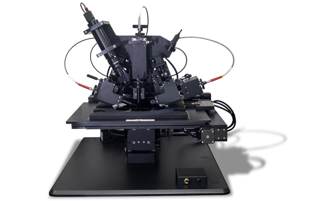
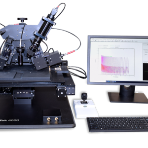
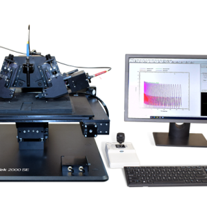
System Components
Standard:
- Spectroscopic ellipsometry with rotating compensator design (295 nm – 1700 nm)
- Multi-angle, polarized spectroscopic reflection (190 nm – 1700 nm)
- Measures film thickness and index of refraction independently
- Multi-Angle Differential Polarimetry (MADP) technology with SCI’s patented Differential Power Spectral Density (DPSD) technology
- Ideal for measuring ultra-thin films (0.03 Å repeatability on native oxide)
- Camera for imaging measurement location
- Pattern recognition
- 50 micron spot size
- Advanced material modeling software
- Bruker’s generalized material model with advanced global optimization algorithms
Optional:
- Generalized ellipsometry (4×4 matrix generalization method) for anisotropy measurements (nx, ny, nz)
- Cassette to cassette wafer handling
- FOUP and SMIF compatible
- Pattern recognition (Cognex)
- SECS/GEM
Related products
Liên hệ
Liên hệ
Liên hệ
Liên hệ
Liên hệ
Liên hệ
Liên hệ
Liên hệ