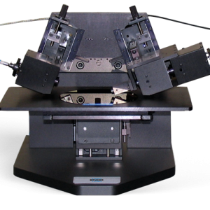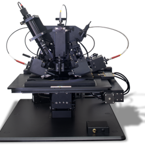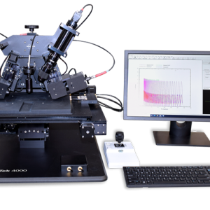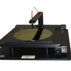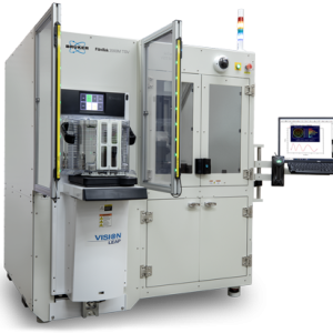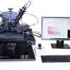


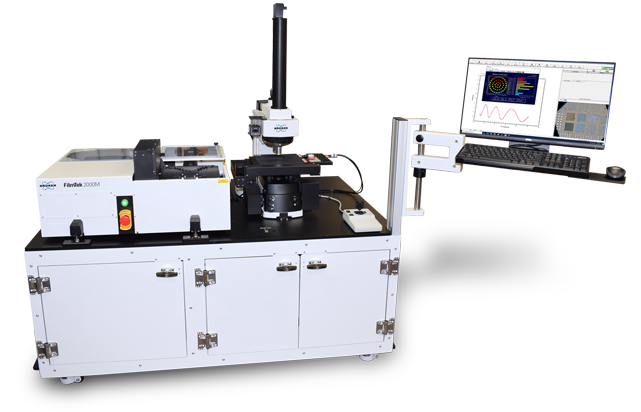
Máy đo phân cực elip và phản xạ FilmTek 2000M
Spectroscopic reflectometry for thickness measurement of thin to very thick films on micron-sized device features
Liên hệ
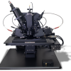
FilmTek 2000M
The FilmTek 2000M™ provides a measurement spot size as small as 1 x 2 µm and a nearly collimated beam. This approach allows accurate, non-contact measurement of thin to very thick films. With automated wafer handling, 1D/2D barcode scanner, and pattern recognition, straightforward measurements from an entire device wafer can be obtained, eliminating the need to infer broader performance from a limited sample area.
Measurement Capabilities
Enables simultaneous determination of:
- Multiple layer thicknesses
- Indices of refraction [ n(λ) ]
- Extinction (absorption) coefficients [ k(λ) ]
- Energy band gap [ Eg ]
- Critical dimension (CD) measurement
System Components
Standard:
- Spectroscopic reflection measurement
- 5nm to 350µm film thickness range
- 2µm spot size (5×10µm standard)
- Automated stage with autofocus
- Camera for imaging measurement location
- Pattern recognition
- Advanced material modeling software
- Bruker’s generalized material model with advanced global optimization algorithms
Optional:
- Automated wafer handling
- SECS/GEM