


NanoWizard® NanoOptics
The NanoWizard® NanoOptics AFM is optimized for a broad range of applications ranging from nanoscale optical imaging by aperture and scattering-type SNOM to experiments involving interactions of light with the sample such as absorption, excitation, nonlinear effects and quenching.
Cutting edge technology to study nanooptical phenomena
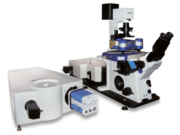
The new NanoWizard® NanoOptics head comes with excellent physical and optical access to the sample from top and bottom as well as from front and side, even when the head and condenser are in place. Additionally, it has an integrated port for fiber SNOM applications.
Because stability and reproducibility of the SPM-tip positioning and scanning are vital for applications requiring the collection of single photons over a long time period, the system has been optimized for it. Improved closed-loop control on 5 or 6 axes and highest scanner resonance frequency in z deliver a scanner performance previously not available in a commercial AFM. This ensures highest data quality for imaging and force measurements in air and liquids.
The new Vortis™ Advanced SPM controller delivers cutting edge values for noise levels, data acquisition speed, and maximum versatility. Advanced electronics and software for multiple feedback controls, highest bandwidth and access to all signals combined with the ability to work with user-written scripts are all key elements for successful experiments. Synchronization of AFM and spectrometer data is achieved by a user-friendly software interface.
The NanoWizard® AFM is designed for optimal use in liquid and comes with a vapour barrier, encapsulated piezos and a variety of dedicated liquid cells. The system may also be used in air or controlled gas environments.
Flexibility in the software and the range of accessories make the system ready for any user-defined experiments. The newly developed fiber coupled detection module for sensitive detectors such as APDs and PMTs delivers outstanding results in terms of stray-light suppression.

Optical near-field experiments
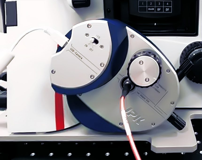
Fiber coupled detection module mounted on a Leica microscope side port.
Aperture fiber SNOM experiments
An integrated fiber SNOM port in the NanoWizard® NanoOptics head and the Tuning Fork module allow hassle-free integration of techniques.
Scattering-type SNOM (sSNOM) experiments
The new system is perfect for tip-enhanced applications such as fluorescence with nano-antennas made of nanofabricated or chemically modified tips. As an alternative to cantilever based optical probes, STM tips can be used with the new Scanning Tunnelling Microscopy (STM) module.
Nanomanipulation in optical fields
The new system is ideal for studying optical surface properties of dyes and markers, quantum dots/rods or metamaterials such as quenching or plasmon generation in combination with topography, nanomechanical, electrical and magnetic properties. Thanks to the symmetric design of stage and head as well as the latest closed-loop scanner technology in a 5- or 6-axis configuration, long-term stability and reproducibility reach the highest possible level.
Key components and basic parameters for Raman/TERS/BioTERS experiments
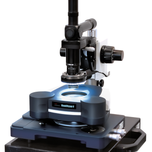
Tip and sample scanner combination
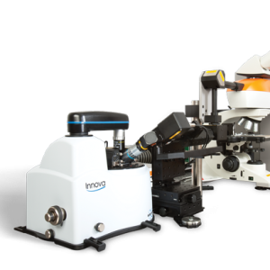
NanoWizard® head (3 scan axes) and TAO™ sample scanner module (2 or 3 scan axes) on top of an inverted microscope integrated into a Raman spectrometer
Suppression of optical cross talk between AFM and Raman excitation/signal
980nm laser source in the AFM
Blocking and cleaning filters in the AFM head
AFM stability over long time
High performance closed-loop scanners and symmetric design of AFM head and stage
Coverslip based fluid cells with temperature control and fluid exchange for highest stability in combination with oil or water immersion objectives
System integration
Synchronization between AFM tip and sample position, and Raman signal recording in the JPK software
JPKs proven algorithm to find the perfect tip position in the focus of the high-NA objective lens
Flexibility
Large variety of AFM/SPM operation modes
Vortis™ Advanced controller with highest speed and lowest noise with a large number of signal channels accessible with the Signal Access front panel
Easy-to-use and fully featured JPK software for advanced experiments for beginners and experts
Raman Reflector Kit for TERS on opaque samples
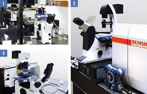
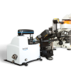
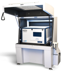
NanoWizard® NanoOptics setup with [1] Acton Advanced SP2750 [2] Renishaw inVia and [3] Jobin Yvon LabRaw HR.
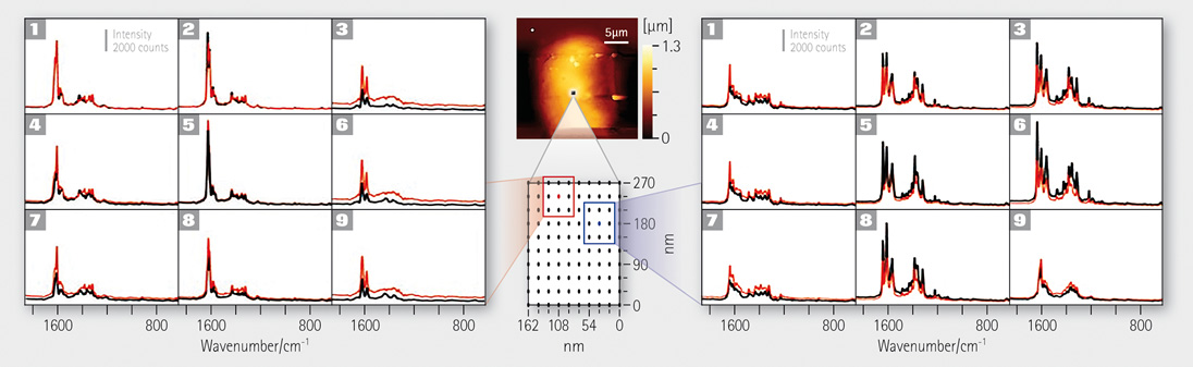
TERS mapping on fixed single human colon cancer cells (HT29 in liquid); Raman data analysis by hyperspectral unmixing algorithm N-FINDR. From: M. Richter, M. Hedegaard, T. Deckert-Gaudig, P. Lampen, V. Deckert: “Laterally resolved and direct spectroscopic evidence of nanometer-sized lipid and protein domains on a single cell”, Small 7(2): 209 (2011).
Advanced fluorescence techniques and Time Correlated Single Photon Counting (TCSPC)
Complementary techniques to AFM, such as epi-fluorescence, confocal laser scanning microscopy, TIRF, FRET, FCS, FLIM, FRAP, STORM, PALM, STED, spinning disc, etc., give insight about the behavior or location of particular features.
It is now possible to routinely combine AFM imaging and force measurements with these optical methods on the same sample spot simultaneously.
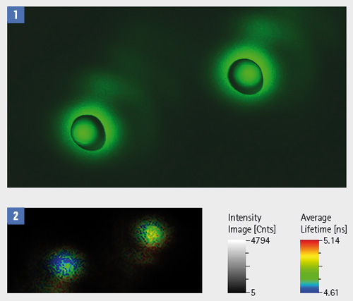
Simultaneous AFM and FLIM measurements on nanoparticles. Scan size 800nm². [1] 3D height information with fluorescence signal overlaid in green. [2] Lifetime signal.
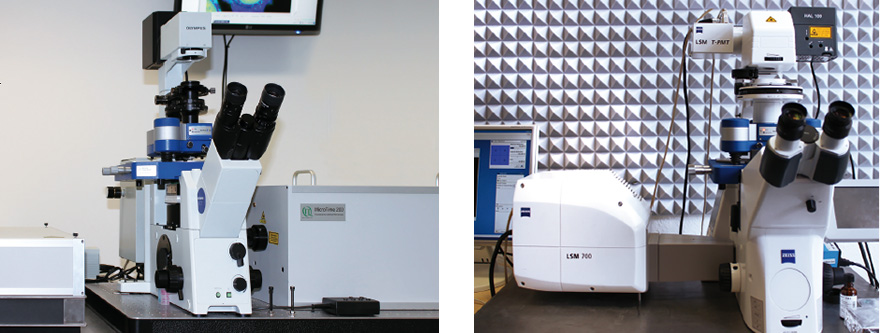
The images show the NanoWizard® AFM combined with a Picoquant MicroTime 200 FLIM system and with a Zeiss LSM 700 confocal
Operating Modes
Standard Operating Modes
Imaging modes
- Easy-to-use and intuitive QI™ mode with precise force control
- Contact mode with lateral force microscopy (LFM)
- AC modes with phase detection
Force measurements
- Static and dynamic spectroscopy
- Advanced force mapping
Optional Modes
- Fast scanning option up to 100 lines/sec
- QI™ Advanced mode for quantitative data
Mechanical properties such as adhesion, elasticity, stiffness, deformation
Conductivity and charge distribution mapping
Contact Point Imaging (CPI) with zero force
Molecular recognition imaging for binding site mapping - HyperDrive™ mode for highest resolution imaging in fluid
- Advanced AC modes such as FM and PM with Q-control & Active Gain Control
- Higher harmonics imaging
- MicroRheology
- Kelvin Probe Microscopy and SCM
- MFM and EFM (see also QI™ mode)
- Conductive AFM (see also QI™ mode)
- STM
- Electrical spectroscopy modes
- Piezo-Response Microscopy
- Electrochemistry with temperature control and optical microscopy
- NanoLithography and NanoManipulation
- Nanoindentation
- Scanning Thermal AFM
- JPK ExperimentPlanner™ for designing a dedicated measurement workflow
- JPK RampDesigner™ for custom designed force curve segments for clamp and ramp experiments
- ExperimentControl™ feature for remote experiment control
- Environmental control options
- DirectOverlay™ for combined AFM and optical microscopy
- Additional xy or z sample movement stages available with CellHesion®, TAO™ and HybridStage™ modul
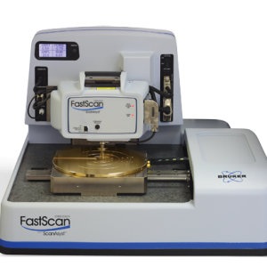
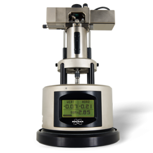
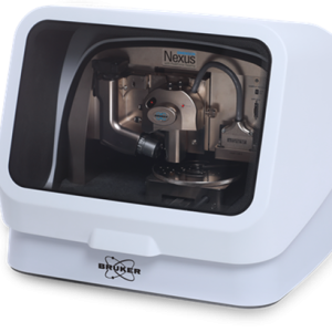
Related products
Liên hệ
Liên hệ
Liên hệ
Liên hệ
Liên hệ
Liên hệ
Liên hệ
Liên hệ
Liên hệ