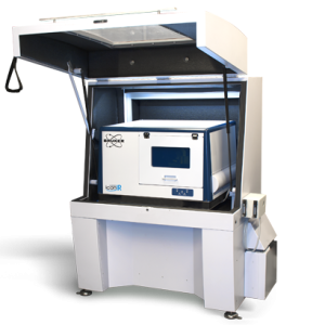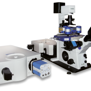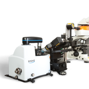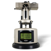


Kính hiển vi lực nguyên tử Dimension XR
Extreme research systems for nanomechanics, nanoelectrical and nanoelectrochemistry
Liên hệ
Dimension XR
Bruker’s Dimension XR scanning probe microscope (SPM) systems incorporate decades of research and technological innovation. With routine atomic defect resolution, and a host of unique technologies including PeakForce Tapping®, DataCube modes, SECM and AFM-nDMA, they deliver the utmost performance and capability. The Dimension XR family of SPMs package these technologies into turnkey solutions to address nanomechanical, nanoelectrical, and electrochemical applications. Quantification of materials and active nanoscale systems in air, fluid, electrical, or chemically reactive environments has never been easier.
Highest Resolution for All Modes, All Environments
From point defects in liquid and stiffness maps to atomic resolution in air and conductivity maps, Dimension XR systems deliver highest resolution in all measurements. They utilize Bruker’s proprietary PeakForce Tapping technology to achieve both hard and soft matter performance benchmarks, including crystal defect resolution and molecular defects in polymers. The same technology plays an equally important role in resolving the smallest asperities on roughened glass over hundreds of images. The systems combine PeakForce Tapping with extreme stability, unique probes technology, and Bruker’s decades of experience in tip scanning innovation. The result is highest resolution imaging consistently, completely independent of sample size, weight, or medium – and for any application.

Revolutionary AFM-nDMA

High-resolution storage modulus map on four-component (COC, PE, LLDPE, elastomer) polymer (left). Storage Modulus spectra collected at individual points (right).
For the first time an AFM can provide complete and quantitative viscoelastic analysis of polymers at the nanoscale, probing materials at rheologically relevant frequencies, in the linear regime. Proprietary dual-channel detection, phase-drift correction, and reference frequency tracking enable a small strain measurement in the rheologically relevant 0.1 Hz to 20 kHz range for nanoscale measurements of storage modulus, loss modulus, and loss tangent that tie directly to bulk DMA.
Proprietary DataCube Modes
These modes utilize FASTForce Volume to perform a force-distance spectrum in every pixel, with a user-defined dwell time. Using high data capture rates, a multitude of electrical measurements are performed during the dwell time, resulting in electrical and mechanical spectra at every pixel. DataCube modes provide full characterization in a single experiment, which is unheard of in a commercial AFM.

Dimension XR’s DataCube modes provide multidimensional nanoscale information at every pixel, simultaneously capturing in a single measurement both electrical and mechanical characteristics.

A DCUBE-PFM measurement clearly shows the domains flipping at different potential levels for each discrete pixel on a BiFeO3 thin film.
Exclusive PeakForce SECM

(A) Bruker’s exclusive premounted PeakForce SECM probes offer easy and safe handling, as well as extremely stable performance over hours of imaging and multiple cleaning cycles. (B) SEM images of the probe; (C) COMSOL simulation of 10 mM [Ru(NH3)6]3+ profile; (D) 1st, 25th, and 50th CVs selected from 50 continuous scans at a scan rate of 20 mV/s; (E) 2-hour amperometric test at -0.1 V versus AgQRE, inset magnification from 70 to 120 min.; and (F) simulated (dashed lines) and experimental (solid lines) approaching curves. C and E images courtesy of C. Xiang and Y. Chen, Caltech.
With a spatial resolution less than 100 nm, this mode redefines what is possible in the nanoscale visualization of electrical and chemical processes in liquid. PeakForce SECM dramatically improves, by orders of magnitude, the resolving power over traditional approaches. This enables entirely new research into energy storage systems, corrosion science and biosensors, opening the door to novel measurements on individual nanoparticles, nanophases, and nanopores. Only, PeakForce SECM provides simultaneous capture of topographic, electrochemical, electrical, and mechanical maps with nanometer-scale lateral resolution.
Powered by the NanoScope 6 AFM Controller
Featuring higher speeds, lower noise, and greater AFM mode flexibility, the NanoScope 6 controller allows users to harness the full potential of our high-performance Dimension and MultiMode AFM systems. This latest generation controller provides unprecedented accuracy, precision, and versatility for nanoscale surface measurements in every application.
NanoScope 6 uniquely enables Bruker AFMs to:
- Operate in more imaging modes than is possible with competing systems, including unique and advanced AFM modes that require complex control and analysis;
- Collect accurate, quantitative data for nanoelectrical and nanomechanical property measurements in every application; and
- Optimize and customize scanning parameters to meet even the most demanding research and industry measurement requirements.