


Hysitron PI 89
Robust, precise, and modular in-situ SEM nanomechanical test instrument
Liên hệ
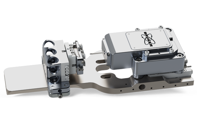
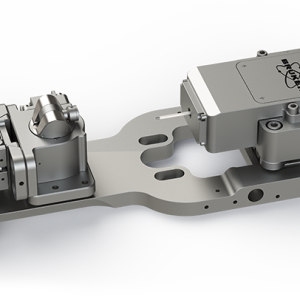
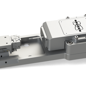
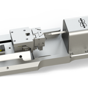
Hysitron PI 89 SEM PicoIndenter
The Hysitron PI 89 SEM PicoIndenter leverages the advanced imaging capabilities of scanning electron microscopes (SEM, FIBSEM, PFIB), making it possible to perform quantitative nanomechanical testing while simultaneously imaging. PI 89 further advances Bruker’s market-leading capacitive transducer technology, which enabled the first commercial in-situ SEM nanomechanics platforms. The new PI 89 Auto adds full automation to four techniques: EBSD, EDS, SEM imaging, and mechanical property mapping.
Techniques available on PI 89 include nanoindentation, tensile testing, pillar compression, particle compression, cantilever bending, fracture, fatigue, dynamic testing, and mechanical properties mapping.
Advanced Performance and Functionality
The compact design of Hysitron PI 89 allows for maximum stage tilt and minimum working distance to enable optimal imaging during testing. PI 89 offers researchers greater versatility and performance than competing systems:
- Redesigned platform increases versatility and ease of use
- 1 nm encoded linear stages provide greater repeatability during automated testing modes while increasing travel range
- Improved frame stiffness (~0.9 x 10⁶ N/m) delivers greater stability throughout the testing process
- Rotation and tilt (RT) stage configurations enable imaging, FIB milling, and access to detectors, such as EDS, CBD, EBSD, and TKD for analytical data and imaging

Two rotation/tilt stage configurations available with next-generation system design. A simple sliding stage added to the system allows quick and simple adjustment of the sample position relative to the transducer.
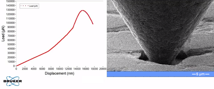
True Displacement Control

Fine load drops in true-displacement control test with SEM PicoIndenter. Rate limiting deformation mechanisms of bcc metals in confined volumes. Acta Materialia, Volume 166, March 2019, p. 687-701, 2019
Hysitron PI 89 utilizes Bruker’s proprietary sub-nanometer sensitivity transducer and piezo-driven flexure for intrinsically displacement-controlled and load-controlled tests:
- In intrinsically displacement-control mode, the piezo actuator can apply displacement with a predetermined displacement rate, and the transducer measures the force
- In true load-control mode, the transducer can apply force electrostatically while simultaneously measuring displacement capacitively
- The uniquely low-current design of the transducer minimizes thermal drift and provides unprecedented load and displacement sensitivity
In-Situ Mechanical Data Synchronized with SEM Imaging and Analytical Mapping
Video capture from the SEM enables real-time monitoring and direct correlation of mechanical data to microscope imaging. Samples were provided courtesy of Professor Steven Nutt, University of Southern California.
In-situ mechanical data acquired with the Hysitron PI 89 are synchronized with SEM imaging and displayed side-by-side. This allows you to see the influence of defects, mechanical strain, and thermal or electrical stimuli on the performance, lifetime, and durability of engineered materials—from nanometer-to-micrometer scales. This synchronization enables a greater range of analyses:
- The rotation and tilt stages of the SEM offer a combination of EBSD and mechanical property mapping of samples
- FIB milling can be performed on a sample before and after nanomechanical testing, without venting a chamber
Automated Co-Localized Imaging and Analysis for High-Throughput In-Situ Nanoindentation
Bruker’s new Hysitron PI 89 Auto SEM PicoIndenter enables full automation of four techniques: EBSD, EDS, SEM imaging, and mechanical property mapping.

PI 89 Auto SEM PicoIndenter
Related products
Liên hệ
Liên hệ
Liên hệ