Quality Control in the electronics and microelectronics industry is confronted with many challenges: A variety of different materials in a sample, some of them metallic and reflective, some matt; a variety of material layers and heights, most often very intricate and hard to discern. Users in microelectronics quality control seek to identify deviations from the standard and improve the production processes so that defects are minimized or even eliminated.
This affects production directly: Samples that exceed tolerances either need to be reworked, or are scrapped directly. The ultimate goal is the continuous improvement of reliability, performance, and efficiency of the deviceDigital microscopes play an important role in inspection and quality control workflows. This image gallery shows typical (micro)electronic samples imaged with the Leica DVM6 digital microscope using different functions like zooming, tilting, tiling, multifocus imaging, different illuminations and contrasting methods, and 3D measurement.
Download your free whitepaper on: Fast and Reliable Inspection of Printed Circuit Boards with Digital
|
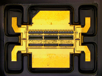
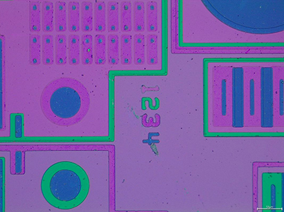
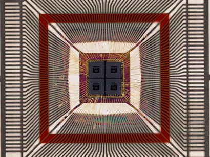
Full overview of a sensor chip with low objective and ring light illumination
|
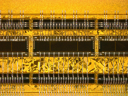
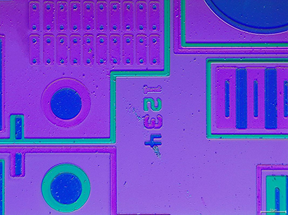
Zoom-in on a sensor chip with middle objective and ring light illumination
|
|
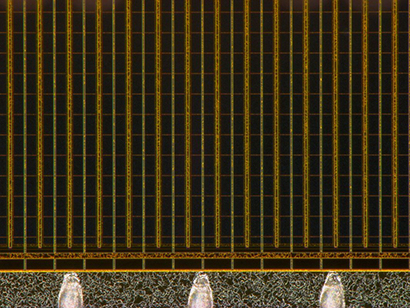
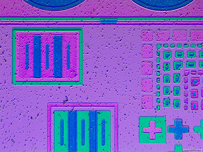
Zoom-in on a sensor chip with low objective and ring light illumination
|
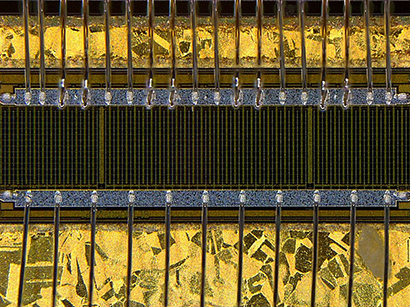
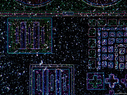
Zoom-in on a sensor chip with middle objective and ring light illumination
|
|
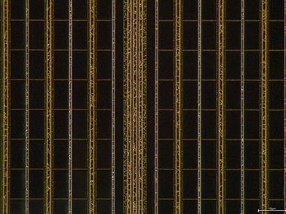
Zoom-in on a sensor chip, 750x
|
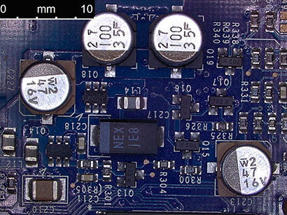
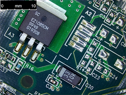
Low magnification overview image of a PCB part
|
|
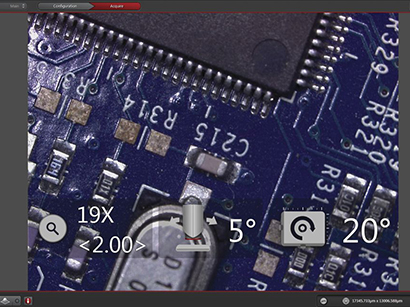
LAS X screenshot of a PCB with 5° tilt at 20° stage rotation-encoding displayed in operation panel
|
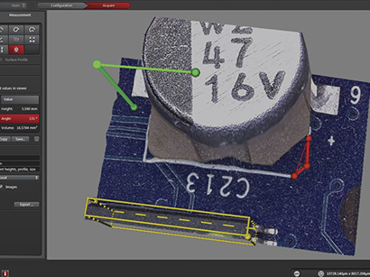
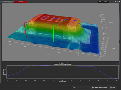
LAS X screenshot of a 3D measurement of a capacitor on a PCB
|
|
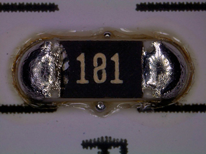
Zoom-in on the soldered ends of a resistor with ring light illumination
|
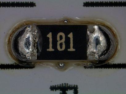
Zoom-in on the soldered ends of a resistor with ring light illumination and a diffusor to reduce glare
|
|
LAS X screenshot showing a 3D typography and measurements in the height profile
|
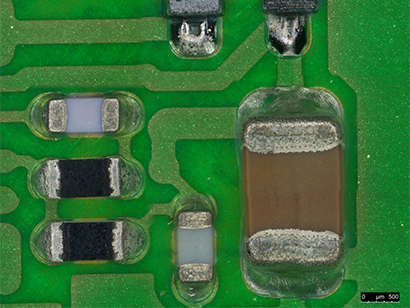
Tile scan of a PCB part with extended depth of field (EDOF) function in LAS X
|
|
Image of a PCB with high-dynamic range (HDR), sample inspection at 30° stage rotation
|
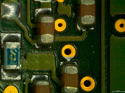
Through hole vias in a PCB inspected with 14° tilt and ring light
|
|
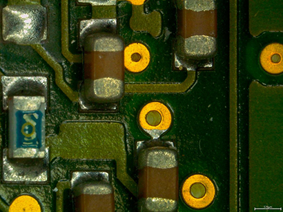
Through hole vias in a PCB inspected with 14° tilt, ring light illumination and backlight adapter
|
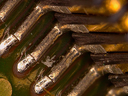
Solderings in a PCB captured with 31° tilt at 43° stage rotation
|
|
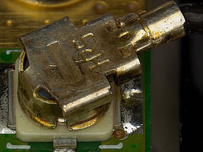
Miniature HF-connector for Wi-Fi antennas used in microelectronic devices
|
Multifocus image of a blind microvia in a PCB, recorded at mag. 650x
|
|
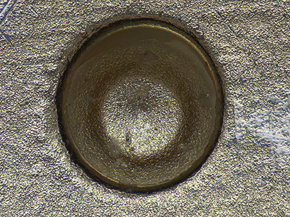
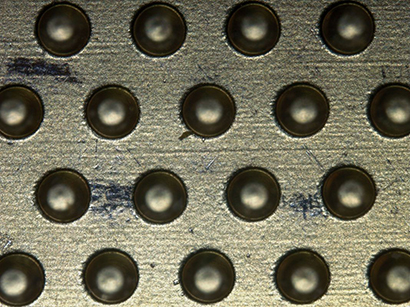
Overview image of microvias in a PCB
|
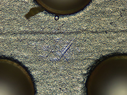
Zoom-in on scratches in a multi-layer-PCB
|
|
Part of a wafer captured with open coax, mag. 750x
|
Part of a wafer captured with open coax and relief contrast, mag. 750x
|
|
Part of a wafer captured with open coax and enhanced relief contrast, mag. 750x
|
Part of a wafer captured with ringlight illumination, mag. 750x
|
|
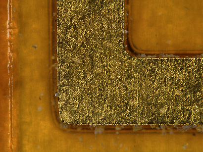
Au-plated Bondpad, Automotive electronics, mag. 120x
|
Zoom-in on Au-plated Bondpad, Automotive electronics, mag. 360x
|
|
Low magnification image of a leadframe, mag. 13x
|
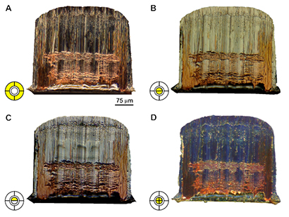
Four views on the cross sections of a Sn-plated copper leadframe with different contrasting options
|
|
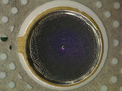
Image of a membrane switch, mag. 60x
|
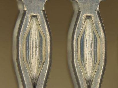
Image of a press fit contact pin of a PCB
|
|
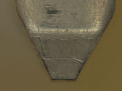
Zoom-in on the tip of a press fit contact pin of a PCB
|
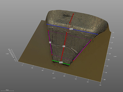
3D measurements on the tip of press fit contact pin with LAS X
|